Trojan detection techniques in hardware implementations
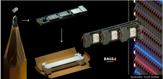
In 2018 we were surprised by the news that Amazon three years ago had begun to quietly evaluate a startup called Elemental, which would be a strategic acquisition to help with the expansion of its streaming video service, now known as Amazon Prime Video. Elemental had created software to compress massive video files and format them for different devices. Its technology had helped broadcast the Olympic Games online, communicate with the International Space Station, and funnel drone footage to the Central Intelligence Agency. AWS, which was overseeing the potential acquisition, hired an outside company to analyze the company's security. First, we looked at their core product: the expensive servers that customers installed on their networks to handle video compression. These servers were assembled for Elemental by Supermicro Computer Inc. which is one of the world's largest providers of server motherboards.
But during the investigation, they found a small microchip, which was not part of the original design of the PCBs. Amazon reported the discovery to US authorities, sending a shudder through the intelligence community. Given that, Elemental's servers can be found in Defense Department data centers, CIA drone operations, and networks aboard Navy warships. Elemental was just one of hundreds of Supermicro customers.
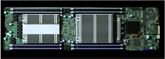 Server baseboard created by Supermicro for Elemental
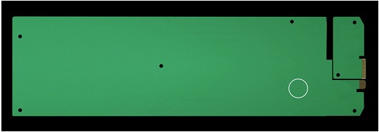 Representation of the Microchip and its location with unknown characteristics and functionalities
The researchers determined that the microchip allowed attackers to create a stealth door into any network that included the hacked servers. The chips are presumed to have been installed in factories run by manufacturing subcontractors in China.
This type of attack was somewhat more serious than the software-based incidents we are used to seeing. Hardware hacks are more difficult to achieve and potentially more devastating, allowing long-term access to any type of company that implements these solutions.
There are two ways to alter the inside of a computer. One, known as interdiction, consists of handling devices that are in transit from the manufacturer to the customer. US spy agencies are favored with this method, according to documents leaked by former NSA contractor Edward Snowden.
The other method involves modifications from manufacturing. One country in particular has the advantage of executing this type of attack: China, which by some estimates makes 75% of the world's mobile phones and 90% of PCs. Even so, to achieve an attack of “sowing” means develop a deep understanding of the design of a product, manipulate it without affecting its functions or components and do it within the factory in record time, and not least ensure that these devices go unnoticed by a large global logistics chain until they reach the desired location.
"Having a well-done, nation-state-level hardware implant surface would be like witnessing a unicorn jumping over a rainbow,” says Joe Grand, a hardware hacker and founder of Grand Idea Studio Inc."Hardware is just so far off the radar, it's almost treated like black magic. ”
Finally, these researchers discovered that eventually this attack of “sowing” affected nearly 30 companies, including a major bank, government contractors, and the world's most valuable company, Apple. Apple was a major Supermicro customer and had planned to order more than 30,000 of its servers in two years for a new global network of data centers. Three senior Apple experts say that in the summer of 2015, malicious chips were also found on Supermicro motherboards. Apple then cut ties with Supermicro the following year, but they described their causes as unrelated reasons.
EThe Chinese government did not directly address questions about the tampering of Supermicro servers, issuing a statement that said, in part, "The Supply chain security in cyberspace is a common concern, and China is also a victim.” The FBI and the Office of the Director of National Intelligence, on behalf of the CIA and NSA, declined to comment.
Today, Supermicro sells more server motherboards than almost any other company in the world. It also dominates the market for PCBs used in special computers, from MRI machines to weapons systems. Their motherboards can be found in custom-built server setups at banks, hedge funds, cloud computing providers, and web hosting services, among other places. Supermicro has assembly facilities in California, the Netherlands, and Taiwan, but it's motherboards are almost all made by contractors in China.
“Think of Supermicro as the Microsoft of the hardware world…” says a former official of US intelligence who studied Supermicro and its business model. "Attacking Supermicro motherboards is like attacking Windows. It’s like attacking the whole world."
Present
Although as of the date of writing this post, almost a decade has passed since the investigation mentioned above and more than half a century since the term Trojan, or rather, Trojan horse, was used for the first time in a report by the Air Force of the USA in graduate “Multics Security Evaluation: Vulnerability Analysis” that mentioned how small blocks of code could affect the hardware of access control systems, posing as something that they were not, currently detecting Trojans in hardware has become a difficulty, since these are no longer only found on an extra “microchip” attached to a PCB, but rather the small transistors that make up the “rogue microchip” could be embedded in the silicon die of the target processors and chipset.
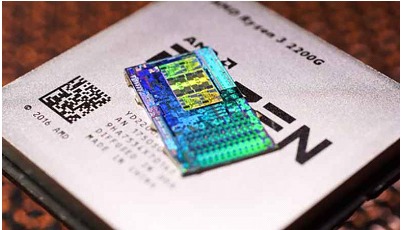 Illustrative Image AMD RAYZEN 3
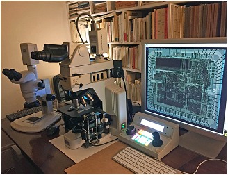
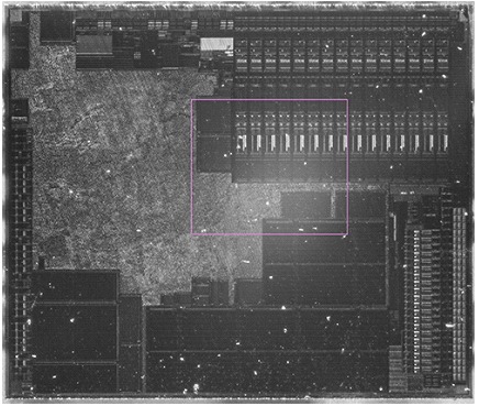
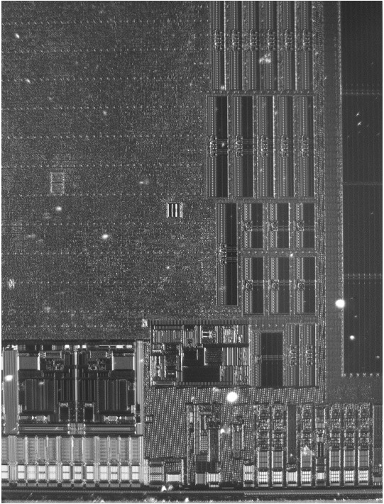
Using thousands of electron microscope images and comparing them to the original chip design, researchers from the Ruhr University Bochum and the Max Planck Institute for Security and Privacy (MPI-SP) have devised an approach to analyzing photos of microchip dies. To reveal Trojan attacks on our hardware, and they are not only having good results but also they are releasing their images and algorithms for any independent researchers to try.
"It’s conceivable that tiny changes might be inserted into the designs in the factories shortly before production that could override the security of the chips…" says Steffen Becker, co-author of the paper detailing the work. "In extreme cases, such hardware Trojans could allow an attacker to paralyze parts of the telecommunications infrastructure at the push of a button."
 High-resolution die shots and original layout files have proven to be enough to automatically flag potentially malicious modifications to CMOS chips.
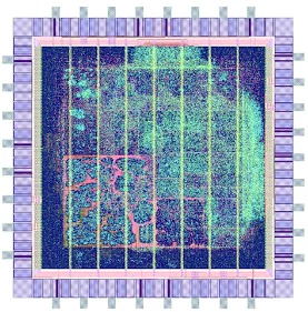
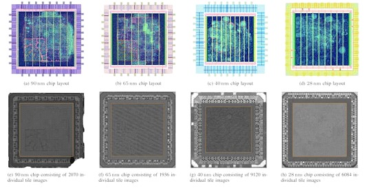
Looking at chips built on 28 nm, 40 nm, 65 nm, and 90 nm processes, the team set about automating the inspection process for such chips. Using designs created by Thorben Moos, they figured out a way to test their approach: "Comparing the chip images and the construction plans turned out to be a big challenge, because we first had to precisely overlay the data," says first author Endres Puschner. "On the smallest chip, which is 28 nanometers in size, a single speck of dust or hair can obscure an entire row of standard cells."
Despite these challenges, the analysis algorithm seemed promising, automatically detecting 37 of the 40 modifications made for the test, including those made to chips built on processes between 40 nm and 90nm. The algorithm certainly returned 500 false positives — but, says Puschner, "with more than 1.5 million standard cells examined, this is a very good rate."
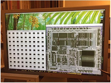
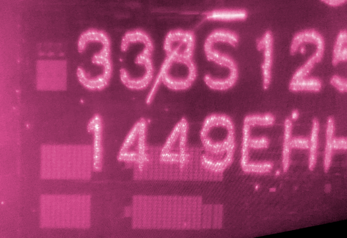
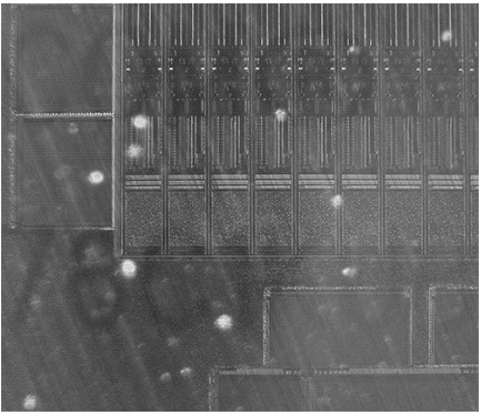
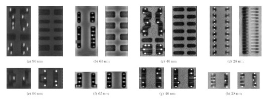 The team's approach picked up the modifications (left) compared to the expected design output (right) automatically.
If you want to carry out your own tests at the end of this post, do not forget to see the references where you can find the team document and the code used that was published on GitHub under the MIT Permissive License.
Current Techniques
Today, there are many options for inspecting chip construction; however, all of these techniques have a “Verification Time vs. Use Time” problem. In other words, none of these techniques is in situ. They should be done on chip samples that are merely representative of the device, or they should be done at remote facilities so that the sample passes through the hands of many strangers before returning to its owner. Scanning Electron Microscopy (SEM), exemplified above, is a popular method of inspecting chips. The technique can produce highly detailed images of even the latest nanometer-scale transistors. However, the technique is destructive: it can only probe the surface of a material. To image transistors, one must remove the top layers of the package through techniques such as decapping down to the metal. Therefore, the technique is not suitable for an on-site inspection.
X-rays, apart from having the corresponding instruments and protections, are not destructive and are capable of carrying out an on-site inspection. However, silicon is almost transparent to the types of X-rays normally used, it can be used to identify the size of the sections and the position of the gold wires that travel from the pads to the silicon die, but cannot give us information about the pattern of the transistors.
On the other hand, X-ray typography is a technique that uses high-energy X-rays that can non-destructively set the pattern of transistors on a chip. The following image is an example of a high-resolution 3D image generated by this technique, as revealed in the paper “High-resolution non-destructive three-dimensional imaging of integrated circuits”
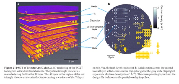
It's a very powerful technique, but unfortunately it requires a building-sized light source, such as the Swiss Light Source (SLS) (donut-shaped building pictured), of which there are few in the world. While it is a powerful method, it is not practical to inspect every device, let alone an end user.

Some companies developed "Portable Laboratories" as is the case of Hamamatsu with its PHEMOS-1000 emission microscope , who describe it as a high-resolution microscope that pinpoints failure locations in semiconductor devices by detecting faint light emissions and heat emissions caused by defects in semiconductor devices. It can be fitted with an optional laser scanning system and allows for the acquisition of high-resolution pattern images.
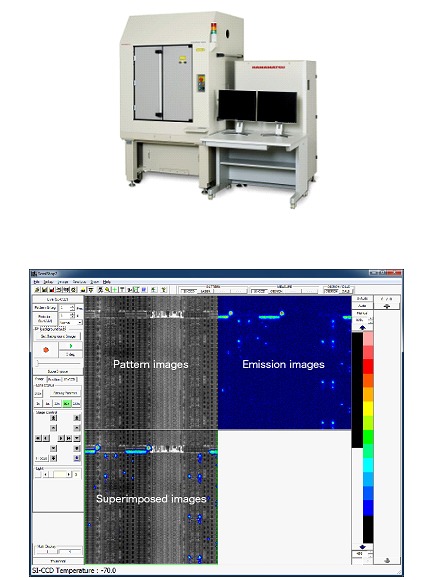 Screenshot of the PHEMOS-1000 software
The latter seems an ideal solution, but unfortunately it is a device that together with its accessories reaches a value of U$D1M, so it is quite restricted to the public.
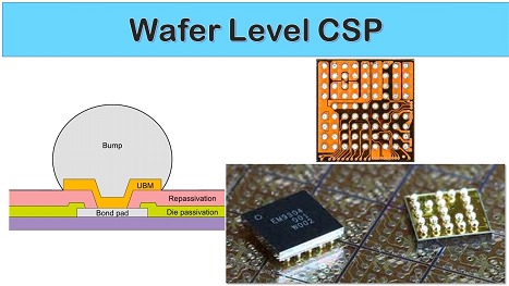
Fortunately, in the chip world, it has become increasingly popular to encapsulate chips without over molded plastic. The downside of exposing delicate silicon chips to potential mechanical abuse is offset by improved thermal performance, better electrical characteristics, and generally lower costs compared to over molding. Due to its compelling advantages, this packaging style is ubiquitous on mobile devices. This type of packaging is commonly known as WLCSP or Wafer-level packaging.
Thanks to this type of packaging and a community with the desire to analyze hardware at the silicon level to detect malicious modifications or counterfeit hardware, driving the manufacture and modification of affordable cost tools for such activities.
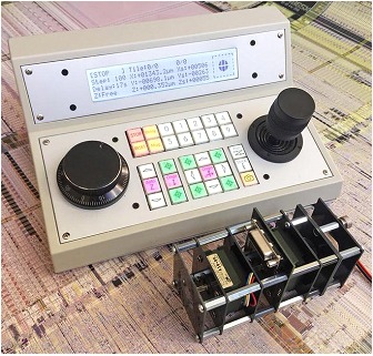 Millimeter motion control for electron microscope developed by the user @Siliconinsid on twitter
The system designs a matrix on the ic and takes a picture for each position assigned by the controller that we saw earlier (this picture is possible by the combination of a microscope biological and a camera) then the photographs are added by software giving a high resolution image of the ic. However, this example is still destructive, given that the photographs are taken on a die without over molding.
IRIS (Infrared, In Situ by Andrew "bunnie" Huang)
But in this post we are going to combine some of the techniques seen previously and above all we are going to base ourselves on a technique by engineer Andrew "bunnie" Huang. Although it lacks of resolution for analysis at the cellular level previously solved with electron microscopes, it yields visible results with conventional microscopes, which is why it was chosen to replicate.
We start with an image of a WLCSP chip in visible light, assembled on a commercially available PCB (in this case, an iPhone 6 motherboard). The scene is flooded with halogen light with almost the entire spectrum visible to the human eye. As a result, the chip appears silvery and dull. Therefore, frontal light microscopy is not suitable for in situ inspection.
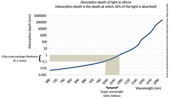
However, an optical study carried out on silicon tells us that it goes from being opaque to transparent in the wavelength range of 1000 nm to 1100 nm (shaded band in the illustration below). Above 1100 nm, it is as transparent as glass; but below 1000 nm, it quickly becomes more opaque.
 Hypothesis
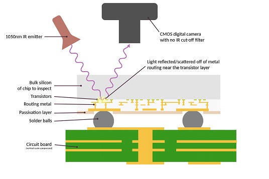
The schematic shows the cross-sectional view of the IRIS inspection setup. The IC just like in real life is already attached to a circuit board and we are lighting the back of the silicon chip. The light is reflected from the metal layers closest to the transistors, and is taken in images with a camera. Conceptually, it's pretty straightforward., but There are some considerations to take into account:
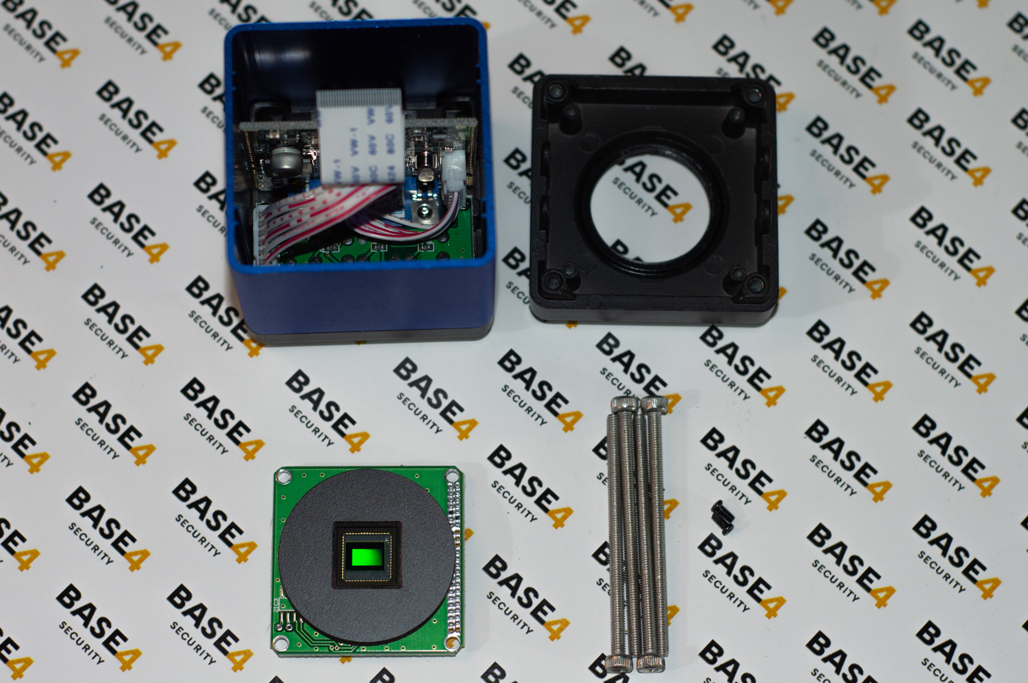
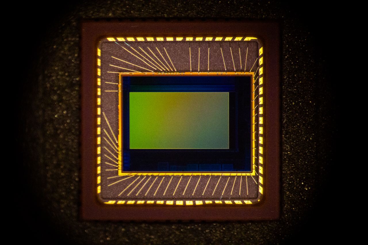 CMOS sensor used in this practice, Photograph taken with Canon 60D
Standard CMOS sensors (the ones used by cameras) retain some sensitivity to shortwave infrared. However, silicon is transparent enough that enough light passes through the bulk silicon layer that forms the back of a WLCSP package for reflected light imaging. More specifically, at 1000 nm, a CMOS sensor might have 0.1x its maximum sensitivity, and a 0.3 mm thick piece of silicon can pass about 10% of the incident light through – so in general we're talking about a reduction ~100x in signal intensity compared to visible light operations. While this reduction is not trivial, it can be overcome with a combination of a stronger light source and a longer exposure time (on the order of several seconds).
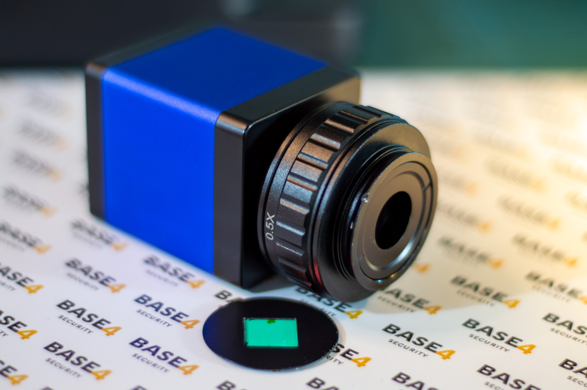
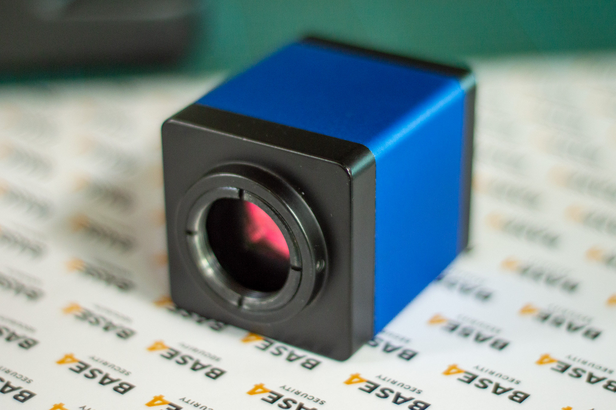 Industrial 12mp digital camera used for testing
But we can improve these results if we remove the IR cut filter from the digital camera. Typically, the extra infrared sensitivity of CMOS sensors is considered problematic, as it introduces color fidelity artifacts. Due to this excess sensitivity, all consumer digital cameras are shipped with a special filter installed that blocks any incoming IR light. Removing that filter is a technique that is used in Astrophotography to be able to capture hydrogen clouds (in reference, I leave the links).
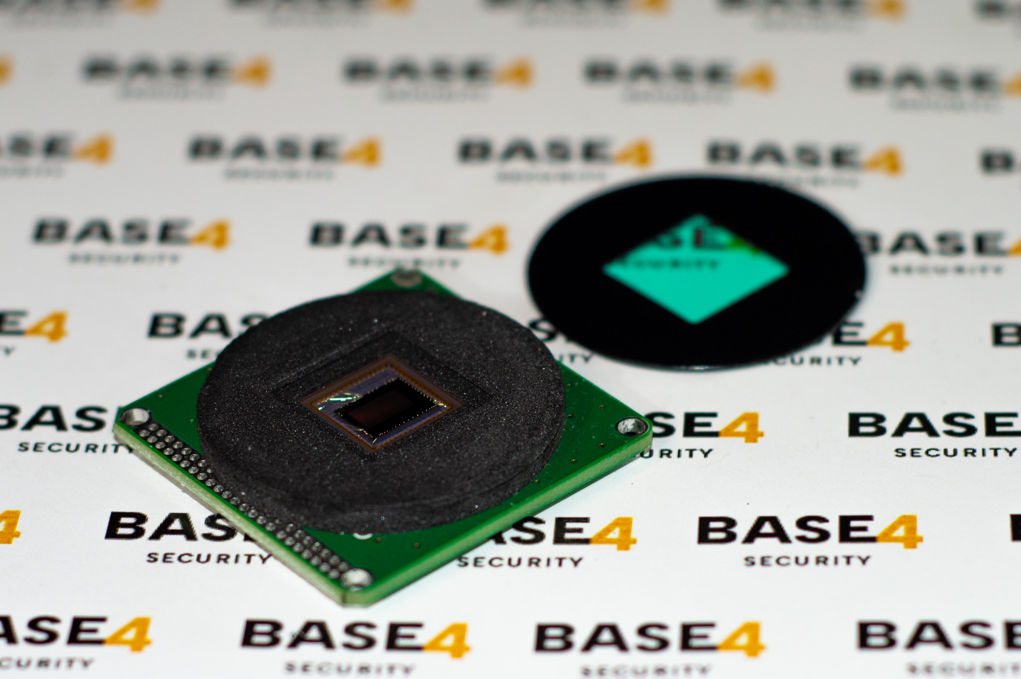 Camera without IR Filter
 Disassembled camera
 Assembled Camera without IR Filter + Focus Adapter Accessory for Microscope
Second, we need an IR light source. Incandescent bulbs and natural sunlight contain a lot of IR light, the current demo setup uses a pair of 1070nm 100mA IF LED emitters, but unfortunately these are not available locally, so we tested with IR lamps intended for Kinesiology and we obtained the following results.
Although these lamps emit at 1050-1070 nm, the excess of other lengths is accidentally reflected on the external surface of the chip and tends to flood the light reflected by the internal metal layers, so the efficiency of the camera decreases too much and the image is poor. Too weak and noisy.
Of course, we could get higher quality images if we invested more money in a source, better optics and a better camera. But theoretically, the results are sufficient.
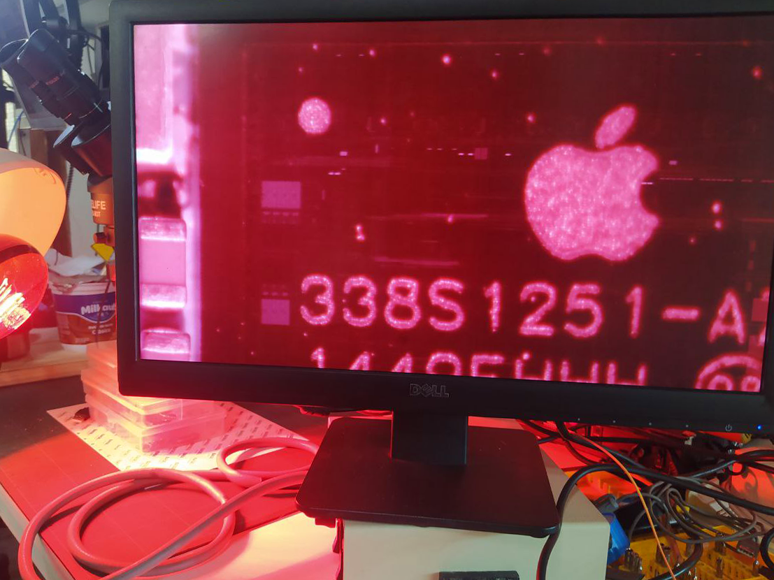
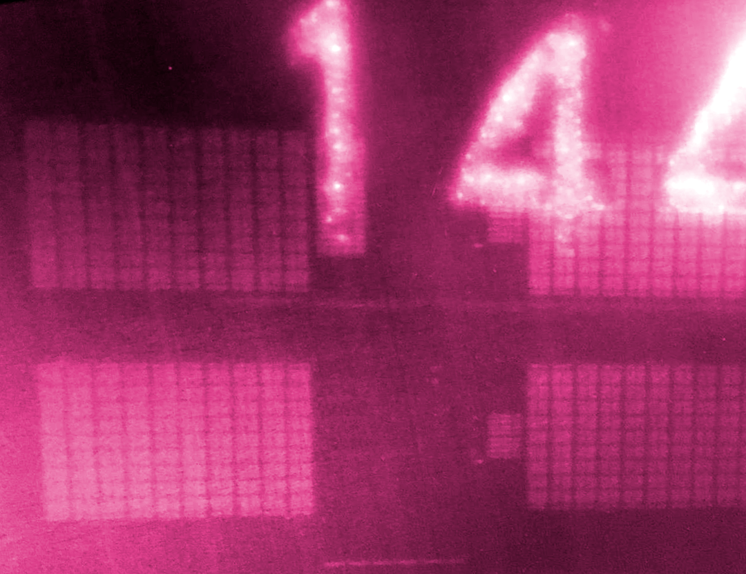
Below are photographs taken by the original researcher:
 Conclusion
IRIS inspection reveals the internal structure of a silicon chip. Fortunately, a fairly wide and popular range of ics already come in WLCSP and FCBGA format and expose the backside of the chips. By itself IRIS cannot inspect the smallest features of a chip, the individual logic gates will be smaller than a micron in height. These cannot be resolved with infrared wavelengths and as such cannot be directly inspected, perhaps by combining SEM techniques, this can be solved. In short, this technique is comparable to being able to X-ray a suitcase at an airport.
As to whether Trojans can be detected Even with improved SEM, malicious changes to chips called “hardware Trojans” can still be really hard to detect, as demonstrated in “Stealthy Dopant-Level Hardware Trojans” byGeorg T. Becker(2013). This Paper proposes that doping modifications would be invisible to most forms of inspection, including SEM, X-Ray ptychography, and IRIS.
The good news is that the attacks discussed (Becker, 2013) are against targets in which it has not been fully hardened against hardware trojans. With a reasonable amount of hardening at the design level, we can increase the logical footprint of a hardware Trojan to something large enough to be detected by IRIS. Fortunately, there is a body of research on hardening chips against Trojans, using a variety of techniques including logical blocking, built-in self-test (BIST) scans, path-delay fingerprinting, and self-authentication methods; all these topics can be found in the book Integrated Circuit Authentication: Hardware Trojans and Counterfeit Detection by Mohammad Tehranipoor, Hassan Salmani, y Xuehui Zhang.
IRIS is a necessary complement to the hardening methods at the logic level, because the hardening methods only logic are vulnerable to bypassing and emulation. In this scenario, a hardware Trojan includes additional circuitry to evade detection by automatically testing for correct responses, such as a wolf wearing a sheep's guise that is donned only when a shepherd is around. Since IRIS can constrain the structure from meso to macro scale, we can rule out medium to large scale circuit modifications, giving us more confidence in microscale verification results as reported by logic-level hardening methods.
Next Steps
IRIS is a promising technique to improve confidence in hardware. With a little forethought and planning, designers can use IRIS in conjunction with logic hardening to gain comprehensive confidence in a chip's integrity from the micro to the macro scale. While the technique may not be suitable for every chip in a system, it is well suited to chip parameters that require high security, such as roots of trust and secure enclaves.
Of course, IRIS is most effective when combined with open source chip design. In closed-source chips, we don't know what we're looking at or what we're looking for; but with open source chips, we can use the design source to augment the capabilities of IRIS to identify features of interest.
Andrew "bunnie" Huang tells us that during the next year, he hopes to improve the core technique of IRIS. In addition to upgrading the optics and adding digital control of the angle and azimuth of the incident light this should play an important role in improving the usability of IRIS. Sub-wavelength features on a chip interact with incident light like a hologram. By modifying the azimuth and angle of illumination, it is likely that we can gain even more information about the structure of the underlying circuitry, even if it is smaller than the diffraction limit of the system. Personally, I believe that the rapid growth of a community, coupled with these techniques, brings us closer to a new era of hardware research that would have seemed like fantasy years ago.
References
- Andrew ‘bunnie’ Huang “Infra-Red, In-Situ (IRIS) Inspection of Silicon”, Sutajio Ko-Usagi Pte Ltd, Singapore.
- “Red Team vs. Blue Team: A Real-World Hardware Trojan Detection Case Study Across Four Modern CMOS Technology Generations”
- Paul A. Karger, 2Lt, USAF, Roger R. Schell, Maj, USAF “Multics Security Evaluation: Vulnerability Analysis”, Deputy for Command and Management Systems (MCI), HQ Electronic Systems Division Hanscom AFB, MA 01730, 19 July 1972.
- Georg T. Becker1 , Francesco Regazzoni2 , Christof Paar1,3 , and Wayne P. Burleson1, “Stealthy Dopant-Level Hardware Trojans” , 1University of Massachusetts Amherst, USA 2TU Delft, The Netherlands and ALaRI - University of Lugano, Switzerland 3Horst G¨ortz Institut for IT-Security, Ruhr-Universit¨at Bochum, Germany.
- Shahin Tajik∗,1, Heiko Lohrke∗,2, Jean-Pierre Seifert1, and Christian Boit2 “On the Power of Optical Contactless Probing: Attacking Bitstream Encryption of FPGAs”1Security in Telecommunications, 2Semiconductor Devices Technische Universität Berlin, Germany
- Heiko Lohrke,1, Shahin Tajik,3,†, Thilo Krachenfels2,Christian Boit1, and Jean-Pierre Seifert2”Key Extraction Using Thermal Laser Stimulation”1Semiconductor Devices Group, 2Security in Telecommunications Group Technische Universität Berlin, Germany 3Florida Institute for Cybersecurity Research University of Florida, USA
- Ger de Graaf and Reinoud F. Wolffenbuttel. “Illumination Source Identification Using a CMOS Optical Microsystem”